







- Solutions for GaN Optical Communication
- Customize graphics according to customer requirements
- Ultra-High Thermal Conductivity for Extreme Conditions
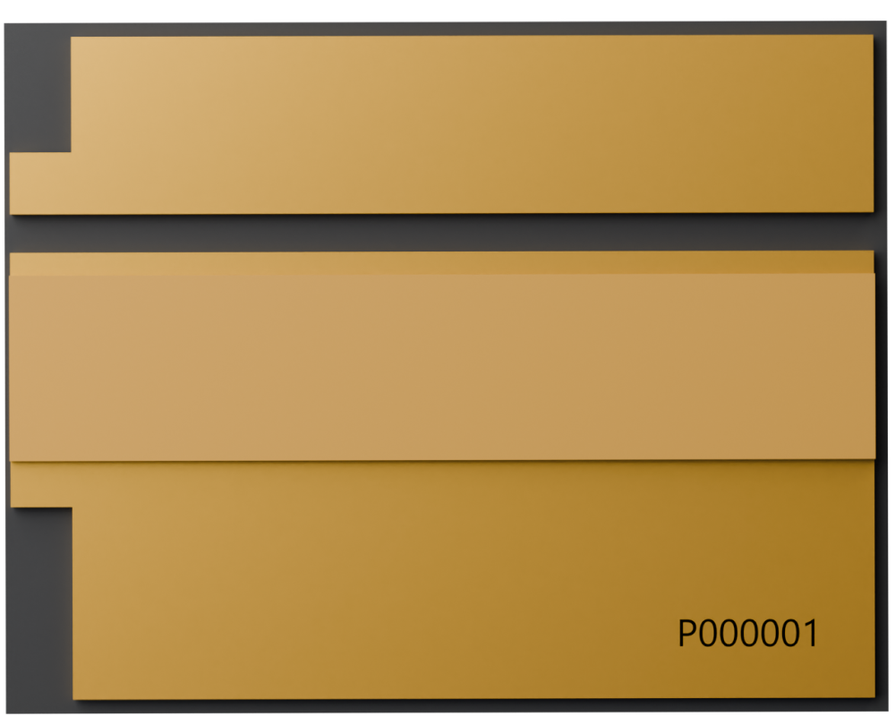
- Multiple Film Architectures Compatible with Varied Package Styles and Current Ratings
- Reliable membrane layer bonding, possessing high reliabilty

| Application Scenario | Power of chip | 5-10W GaN chip | |
| Product Category |
1.Ceramic Submounts for 3D Structured Light Applications 2.High-Power LED Submounts |
||
| Solution | Project | Specification | |
| Ceramic Substrate | Material | Diamond | |
| Thickness | 0.15~0.4mm | ||
| Thermal Conductivity | 1000/2000w/m· K | ||
| Metallization | Composition | Ti/Pt/Au/Ti/Cu/Ni/Au | |
| Thickness |
Ti/Pt/Au=0.1/0.2/0.3-10.0um Ti/Cu/Ni/Au=0.1/10-100um/1-5 um/0.3-2um |
||
| Solder | AuSn | ||
| Ratios of Solder | Au 80 ± 5% Sn 20 ± 5% (customizable) | ||
| Thickness of Solder | 1.5~7um (customizable) | ||
| Pattern Ability | L/S=5um/5um (Thin‑film Products) L/S=25/25um (Heavy‑copper Products) (customizable) | ||
| Other | Cutting Tolerance | ±50um | |
- Product application
- Applications
In the automatic production line, laser cutting and welding are common processing technologies. The ceramic heat sink can effectively manage the heat of laser, ensure the stability and durability of the equipment under high-load operation, and improve the precision of cutting and welding. The laser sensor plays a key role in automatic detection. The ceramic heat sink can maintain the temperature stability of laser emitter, ensure the measurement precision in the detection process, and is applicable to dimension measurement, surface detection, etc.