







- R&D Technology
- Submount R&D Capabilities for Chip Packaging Applications
PGT has established a comprehensive R&D system addressing the requirements of chip thermal management, packaging interconnects, and long-term reliability, covering material selection, structural design, simulation and analysis, sample fabrication, COS evaluation, and reliability validation.
Using customer chip characteristics and packaging applications as key design inputs, and leveraging simulation analysis and actual COS assembly evaluation as core validation methods, PGT enables a closed-loop development process from solution design through mass-production introduction.
R&D Process
-
- 01
- Application Requirements Analysis
-
- 02
- Material & Metallization Selection
-
- 03
- Structural Design
-
- 04
- Simulation & Analysis
-
- 05
- Sample Fabrication
-
- 06
- COS Evaluation
-
- 07
- Reliability Validation
-
- 08
- Design Optimization
-
- 09
- Mass-Production Introduction
-
01Structural Design & Simulation Analysis
-
02COS Assembly & Application Evaluation
-
03Material Characterization & Selection
-
04Multiple Metallization Processes
-
05Sample Fabrication & Rapid Validation
-
06Reliability Validation & Failure Analysis
-
07Customization Capabilities
Structural Design & Simulation Analysis
Customized Design Based on Chip and Packaging Applications
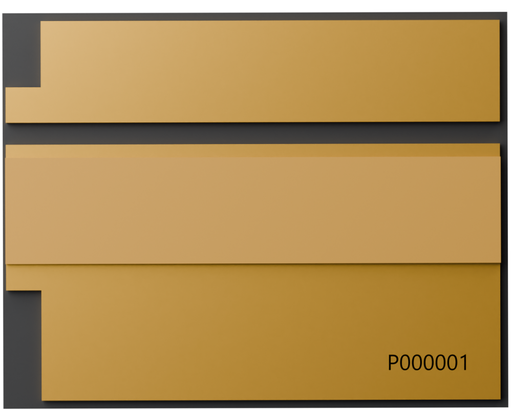
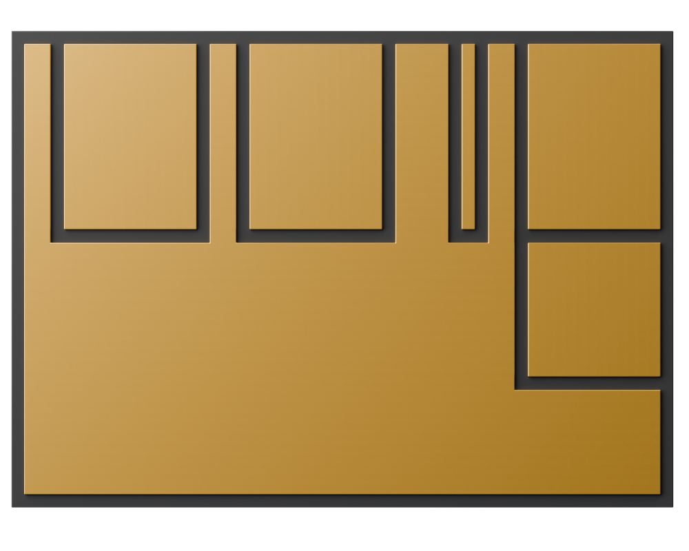
Based on customer requirements including chip dimensions, power density, bonding method, package structure, and operating conditions, PGT develops customized designs for submount patterns, metallization structures and thicknesses, positioning features, soldering areas, and other critical features.
Thermal Performance & Packaging Stress Simulation
Thermal conduction analysis, thermo-mechanical coupled analysis, and finite element analysis (FEA) are applied to evaluate submount structures and chip packaging systems. Simulation results guide material and structural design selection, while actual COS assembly is used for validation and refinement, establishing a closed-loop Design → Simulation → Validation → Optimization development process.
-
- 01
- Application-Driven Design
-
- 02
- Simulation-Guided Development
-
- 03
- COS-Based Compatibility Validation
-
- 04
- Data-Driven Optimization
- Fifteen Core Technologies
- Technical Capability
- Providing contract manufacturing services for various technologies.
-
- PVD (Ceramic Metallization)
- Magnetron Sputtering is a Physical Vapor Deposition (PVD) technology. Plasma confined by a magnetic field bombards the target material, ejecting atoms that are subsequently deposited onto the substrate surface to form a thin film, enabling high-quality ceramic metallization.
-
- Thick Copper Electroplating
- Metal is deposited through an electrochemical process to build up a thick metal layer, providing excellent thermal performance, electrical conductivity, and mechanical properties.
1. PGT has established a correlation model between microstructure and material performance. By controlling the crystalline morphology through optimized processes, superior physical and chemical properties of the plated layer can be achieved.
2. Thick-plating capability supports metal layer thicknesses of over 100 μm.
3. Excellent adhesion of the plated layer, capable of passing extreme high-temperature testing at 350°C for 1 hour.
-
- Nickel/Gold Electroplating
- Nickel and gold layers are deposited through an electrochemical process. The resulting Ni/Au coating provides excellent corrosion and wear resistance, extending product service life while delivering superior solderability and reliability.
-
- Planarization
Grinding and polishing processes are applied to optimize the flatness and surface roughness of the copper layer, providing a high-quality mounting surface for chip packaging.
1. Flatness: <2μm
2. Nanometer-level mirror surface finish achievable
-
- Vacuum Evaporation (Pre-Applied AuSn Solder)
- Evaporation / Vacuum Evaporation is a Physical Vapor Deposition (PVD) technology. Under high-vacuum conditions, the source material is heated until it vaporizes. The vaporized atoms or molecules are transported to the substrate surface and condensed to form a thin film.
-
- Wet Pattern Transfer (Developing, Etching & Stripping – DES)
- Wet chemical processes are used to develop, etch, and strip the photoresist after exposure, transferring the designed pattern onto the thin-film metallization layer to form the required circuit pattern.
-
- Photoresist Patterning (Pattern Transfer)
- Photoresist patterning is a core semiconductor manufacturing process that precisely transfers circuit patterns from a photomask onto a wafer or substrate surface. The process is fundamentally based on a photochemically induced change in photoresist solubility.
-
- Dry Etching (Micro/Nano Fabrication)
- Dry etching is a micro/nano fabrication technology that selectively removes material in a gaseous environment using plasma or high-energy ion beams. The process combines chemical reactions and physical ion bombardment to achieve precise material removal.
-
- Lift-off Process ( Additive Metal Patterning )
- The lift-off process uses patterned photoresist followed by metal deposition. The photoresist and the metal deposited on top of it are subsequently removed, leaving the desired metal pattern precisely defined on the substrate.
-
- Blade Dicing
- Blade dicing is a precision cutting process that uses a high-speed rotating diamond blade to mechanically cut wafers or substrates into individual dies or components. The process is based on precision grinding and material removal of brittle materials.
-
- Laser Dicing
- Laser dicing uses a high-energy-density laser beam to rapidly melt, vaporize, or ablate material, enabling precise material separation. The process is based on a coupled optical-thermal-mechanical material removal mechanism.
-
- AOI & Sorting (Automated Optical Inspection & Sorting)
AOI:
Automated Optical Inspection (AOI) is a non-contact automated inspection technology based on optical imaging and image-processing algorithms. High-resolution cameras capture product surface images, which are compared against reference templates or algorithmic models to automatically identify and classify defects.
Die Sorting / Pick-and-Place:
The die sorter is a key piece of equipment in semiconductor back-end processing. It picks individual dies from dicing tape (blue tape/UV tape) and sorts them according to AOI inspection data into designated trays or tubes. The system integrates high-precision vacuum pick-up, vision positioning, and motion control.
-
- Packaging & Testing Platform (COS / COC / TO)
- 1. Submount Performance & Quality Monitoring Platform
2. Failure Analysis Platform
3. Product Evaluation & Alternative Qualification Platform
-
- Reliability Platform (Reliability Testing)
The reliability platform serves as a central hub for quality validation and risk screening throughout the entire product lifecycle. Its core mission is to identify potential failures before shipment, monitor process drift during mass production, and validate lifetime limits during the design stage.
Testing capabilities cover environmental stress testing, electrical stress testing, and mechanical stress testing.
-
- Pre-Applied Solder on Housings (Package Housings)
- For laser package housings, PGT provides customized integrated solutions with pre-applied solder, reducing precious-metal consumption and customer-side assembly steps while improving soldering reliability. The solution also supports lightweight material innovations, delivering cost savings and improved manufacturing efficiency.
- Inspection and Testing Platform/Capability
- Detection Capability
-
Characterize material properties through various physical and chemical measurement methods to support the design of the overall product structure.
- Measurement methods include:
- Thermal Analysis Characterization
- - Thermal conductivity measurement (thermal conductivity tester)
- - Coefficient of thermal expansion (TMA)
- Microstructure Morphology Characterization
- - SEM observation (EBSD analysis)
- - Step height measurement (profilometer)
- - 3D optical measurement
- Mechanical Performance Characterization
- - Flexural strength (universal testing machine)
- - Push-pull force testing
- PGT Laboratory
- COS Packaging and Testing Platform Laboratory
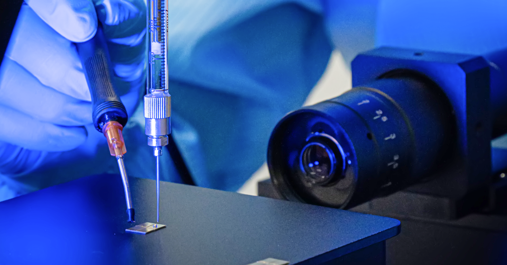
- Built around actual customer and industry packaging applications, PGT has established comprehensive packaging and testing capabilities covering COS, TO, COC, adhesive die bonding, and other packaging processes, with three core missions:
- 01Ensuring delivery quality
- 02 R&D iterative closed-loop
- 03Failure mode analysis
-
- High-Precision Eutectic Bonding Platform
- Bonding Accuracy: ±3 μm
Pulse Heating
Bonding Force Control
Nitrogen Atmosphere Protection
-
- Gold Wire Bonding
- Equipped with industry-leading advanced wire bonding equipment, enabling high-reliability bonding with 1 mil gold wire.
-
- Packaging Inspection
- Comprehensive packaging reliability inspection, including low- and high-magnification microscopic inspection, OH measurement, warpage measurement, die shear and wire pull testing.
-
- Optoelectronic Testing
- Stable temperature control with comprehensive optoelectronic performance testing capabilities for COS, COC, and TO modules, including LIV and spectral testing.
-
- Failure Analysis
- Professional inspection and failure analysis for both internal and customer products, with comprehensive capabilities covering CP, FIB, XPS, SEM, EDX, C-SAM, 3D surface profiling, 3D X-ray inspection, and other advanced analytical techniques.